Ball Grid Array (BGA) packages have become essential in modern electronics because they provide high interconnection density without requiring excessive PCB area. Processors, FPGAs, memory devices, and communication ICs frequently use BGA packaging to accommodate hundreds or thousands of electrical connections.
However, the same packaging architecture that makes BGAs attractive also creates significant manufacturing challenges. Unlike conventional leaded components, BGA solder joints are hidden beneath the package. Their quality depends on the interaction between solder metallurgy, package warpage, PCB pad geometry, thermal behaviour, and reflow process conditions.
A BGA can pass initial electrical testing and still contain weak or partially formed joints that fail after thermal cycling or mechanical loading. Understanding these failure mechanisms is essential for improving assembly yield and long-term reliability.
Understanding BGA Solder Joint Formation
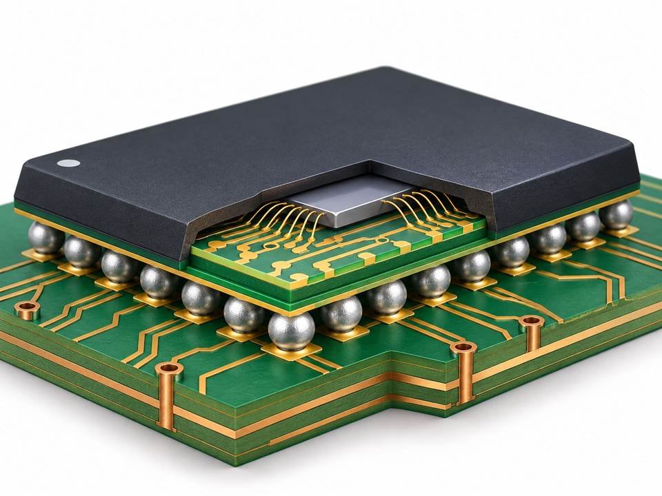
During reflow soldering, the solder balls attached to a BGA package interact with solder paste deposited on the PCB pads. As the assembly reaches the solder alloy’s melting range, the solder becomes liquid, flux removes surface oxides, and the molten solder wets the appropriate metallized surfaces.
A properly formed joint develops metallurgical bonds through the formation of intermetallic compounds (IMCs) at the interfaces. For common lead-free SAC alloys, these reactions typically involve tin and the metallization present on the package and PCB pads.
The final joint geometry depends on solder volume, pad dimensions, surface tension, and the separation between the package and board. If the solder cannot wet properly, if the package lifts away from the PCB during reflow, or if solder volume is insufficient, the joint may be defective.
1. Head-in-Pillow Defects and Incomplete Solder Coalescence
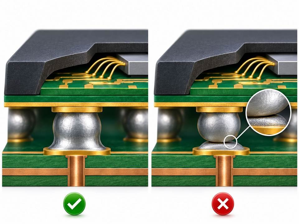
Head-in-Pillow (HiP) is among the most challenging BGA soldering defects because it can produce an electrical connection without establishing a reliable metallurgical bond. The defect occurs when the BGA solder ball and printed solder paste fail to fully coalesce during reflow. After cooling, the ball may rest against the solder deposit, creating a shape resembling a head pressed into a pillow.
How Head-in-Pillow Develops
Two mechanisms are particularly important. The first is inadequate wetting. Oxidation, contamination, or insufficient flux activity can prevent the molten solder surfaces from merging.
The second is dynamic package or PCB warpage. During heating, differences in thermal expansion may cause the package to deform and temporarily separate some solder balls from their corresponding pads. If separation occurs while solder is molten, oxidation or changes in solder geometry may prevent proper coalescence when contact is restored.
Research published through IPC identifies both poor wetting and warpage as major contributors to Head-in-Pillow defects. These mechanisms can also interact, making root-cause analysis more complicated.
Why HiP Escapes Electrical Testing
A defective joint may maintain temporary electrical contact through mechanical pressure between the solder ball and deposit. Consequently, a board may pass a basic continuity test. However, vibration, board bending, or temperature changes can disturb the interface and create intermittent opens.
This makes Head-in-Pillow especially concerning for automotive electronics, industrial control systems, and products exposed to repeated thermal or mechanical stress.
2. Package Warpage During Reflow
BGA packages contain materials with different coefficients of thermal expansion (CTE), including silicon, organic substrates, mold compounds, and copper structures. As temperature changes, these materials expand and contract at different rates. The result can be dynamic package warpage.
A package that appears flat at room temperature may develop substantial curvature near peak reflow temperature.
How Warpage Affects Solder Joint Geometry
Depending on the direction of curvature, certain solder balls may move away from their PCB pads while others experience increased compression. Excessive separation can prevent adequate solder contact and contribute to HiP or non-wet opens. Conversely, excessive compression combined with solder volume or placement problems may increase bridging risk.
Warpage can produce nonuniform joint heights across the package. The problem becomes more difficult as packages become larger, thinner, and more densely populated.
A study published in Materials Transactions examined the relationship between package warpage and Head-in-Pillow formation, demonstrating the importance of thermomechanical deformation during reflow.
Controlling Warpage-Related Failures
A proper investigation should consider package characteristics, board support, component storage conditions, and the reflow profile. When necessary, warpage measurements should be performed at elevated temperatures rather than relying exclusively on room-temperature measurements.
The assembly’s thermal profile must also stay within component and material specifications. Simply increasing peak temperature is not a universal solution; it may improve wetting in one situation while increasing package deformation or thermal damage in another.
3. Solder Voids and Internal Joint Discontinuities
Voids are gas-filled cavities within a solder joint. They can develop when volatile materials become trapped as solder solidifies. Potential sources include flux outgassing, moisture, surface contamination, and gases generated during heating.
Small voids are relatively common in soldering processes, and their presence does not automatically indicate an unacceptable assembly. The engineering concern is their size, location, distribution, and effect on the joint’s mechanical or thermal performance.
Why Void Location Matters
A void near a highly stressed interface may influence crack initiation more significantly than a similarly sized void near the center of a solder joint. Large or interconnected voids can reduce the effective load-bearing solder area.
However, reliability cannot be predicted accurately from void percentage alone. Joint geometry, alloy composition, loading conditions, and the applicable acceptance criteria must also be considered, particularly near intermetallic layers where cracks may initiate or propagate.
Reducing Voiding During Assembly
Voiding should be investigated as a process issue rather than addressed through a single parameter adjustment. Relevant variables include solder paste chemistry, stencil design, pad finish, surface cleanliness, and reflow conditions.
Extended exposure at elevated temperature may promote volatile removal in some circumstances, but excessive thermal exposure can also degrade flux performance or increase oxidation. Process optimization requires balancing these competing effects.
4. Non-Wet Opens and Poor Surface Wetting
Non-Wet Open (NWO) defects occur when solder fails to establish the intended wetting and metallurgical connection at an interface. Although closely related to HiP, the underlying failure may involve insufficient wetting of a pad or solderable surface rather than incomplete coalescence between two solder masses.
Possible contributors include oxidized pads, contaminated component terminations, inadequate flux activity, and unsuitable reflow conditions. Surface finish quality also matters.
PCB finishes such as ENIG, OSP, and immersion silver provide different solderability characteristics and storage requirements. For example, improper processing of an ENIG finish can introduce interface defects that affect joint integrity. Such failures require metallurgical investigation rather than assuming that solder paste or the reflow profile is solely responsible.
Distinguishing Wetting Problems from Mechanical Separation
A useful failure analysis examines the fracture interface and remaining solder distribution. If a joint separates cleanly at a poorly wetted surface, the evidence differs from a joint that formed properly and later fractured through thermal fatigue.
Microscopy, cross-sectioning, and material analysis can help distinguish these mechanisms. Correctly identifying the mechanism is necessary before implementing corrective action.
5. Thermal Fatigue and Long-Term Solder Joint Cracking
Not all BGA failures originate during assembly. Some joints form correctly and later fail because of repeated mechanical strain. Thermal cycling is a common source of this strain.
When the PCB and BGA package have different effective CTEs, temperature changes produce relative displacement between package and board. The resulting deformation is transferred to the solder joints. Over repeated cycles, accumulated inelastic strain can initiate fatigue cracks.
Why Corner Balls Are Often Vulnerable
For an idealized package-to-board CTE mismatch, relative displacement generally increases with distance from the neutral point. This relationship is commonly described using distance to neutral point (DNP).
Corner solder joints often experience relatively high thermomechanical loading because they are farther from the package’s central neutral region. However, actual strain distributions also depend on package stiffness, board construction, solder geometry, and local mechanical constraints.
Cracks may initiate within bulk solder or near intermetallic interfaces. As damage accumulates, electrical resistance may increase or the joint may eventually become open.
Mechanical Loading Compounds the Problem
Board bending, shock, vibration, and enclosure-induced stress can accelerate degradation. Large BGA packages mounted near unsupported PCB regions may experience additional mechanical strain.
Where appropriate, engineers may use mechanical support, revise component placement, or evaluate underfill materials. Underfill can improve reliability in selected applications, but it changes stress distribution and reworkability and must be qualified for the assembly.
6. How X-Ray Inspection Helps Identify Hidden Defects
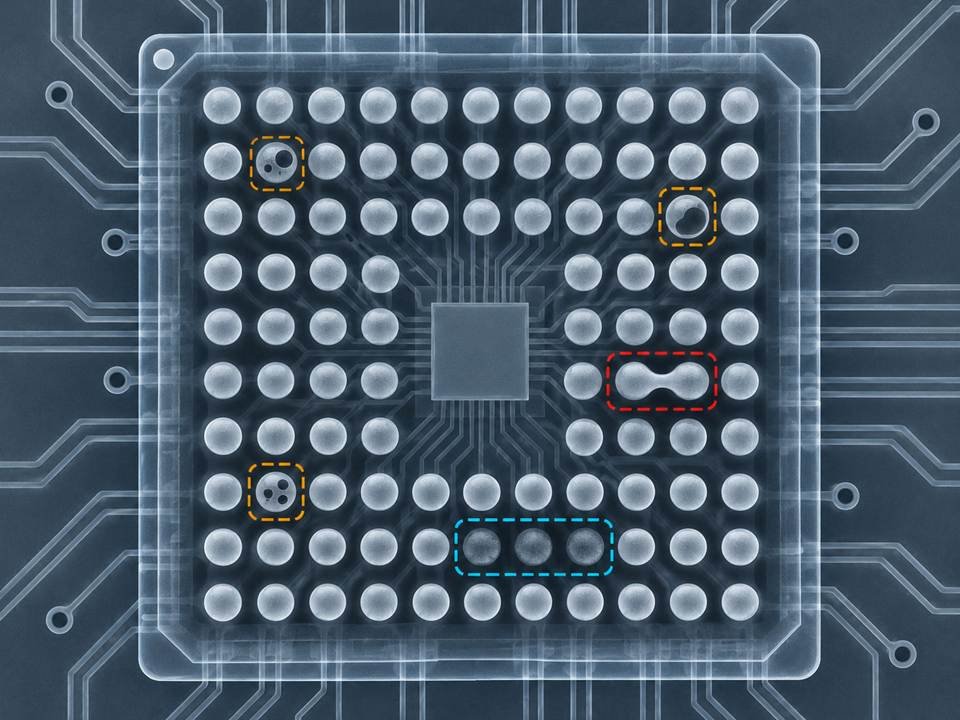
Because BGA connections are beneath the component body, standard visual inspection and automated optical inspection cannot directly examine complete solder joint geometry. X-ray inspection provides a non-destructive method for evaluating hidden solder structures.
Conventional 2D X-ray imaging can reveal many voids, solder bridges, missing balls, and abnormal joint patterns. Angled imaging provides additional information about joint shape and apparent separation. More advanced computed tomography can help resolve overlapping structures and support detailed failure investigations.
For a broader explanation of the available techniques and their applications, this technical guide to PCB X-ray inspection discusses how imaging methods are used to evaluate hidden solder connections in PCB assemblies.
X-Ray Inspection Has Important Limitations
An X-ray image shows differences in material attenuation, not the complete mechanical or metallurgical condition of a solder joint. A joint may appear geometrically acceptable while containing an incomplete metallurgical bond.
Certain Head-in-Pillow defects can be difficult to distinguish using conventional top-down 2D imaging. Similarly, X-ray inspection cannot establish the fatigue life of a solder joint.
For ambiguous failures, engineers may need additional methods such as:
- Cross-sectional microscopy to examine joint interfaces.
- Scanning electron microscopy and EDS to investigate fracture surfaces and material composition.
- Electrical continuity monitoring during thermal or mechanical loading.
- Dye-and-pry analysis, where appropriate, to help identify separation locations.
Inspection results should always be interpreted together with failure symptoms and process history.
7. Reflow Profile Optimization and Process Control
A reflow profile affects solder wetting, package deformation, flux behavior, and final solder joint structure. In lead-free SAC processes, the profile typically includes preheating, a region approaching reflow, time above liquidus, peak temperature, and controlled cooling. Each stage influences joint formation.
Time Above Liquidus and Peak Temperature
For SAC305 solder, the nominal melting range is near 217–220°C, although processing requirements depend on paste formulation and component specifications. Time above liquidus must be sufficient for solder wetting and joint formation.
An excessively short interval may contribute to incomplete wetting. An excessively long interval can increase thermal exposure, influence intermetallic growth, and potentially degrade assembly quality.
Likewise, peak temperature must provide sufficient thermal energy without exceeding component processing limits. A profile should be measured on a representative populated assembly, including locations with different thermal masses. Oven setpoints alone do not establish actual solder joint temperature.
Why a Single Profile May Not Fit Every Board
Large copper areas, thermal vias, ground planes, component density, and board thickness create thermal differences across the assembly. A BGA near a high-thermal-mass region may experience a different temperature history from smaller components elsewhere.
Thermocouple placement and representative profiling are critical. For difficult assemblies, process engineers should examine both coldest and hottest relevant locations and verify that the assembly remains within the allowable window.
8. PCB Pad Design and Solder Volume Control
BGA reliability also depends on pad geometry and solder volume available to form each joint. Common configurations include non-solder-mask-defined (NSMD) and solder-mask-defined (SMD) designs. These influence wetting geometry, solder spread, and local stress distribution.
Neither approach is universally superior for every package. Appropriate design depends on component manufacturer recommendations, board fabrication capability, and assembly process.
Stencil Design and Paste Transfer
Stencil aperture dimensions influence the amount of solder paste deposited on each pad. Insufficient paste may contribute to poor joint formation or opens, particularly when combined with warpage. Excessive paste can contribute to bridging or unfavorable joint geometry.
Paste transfer efficiency becomes increasingly important as aperture dimensions decrease. Engineers should consider stencil thickness, aperture area ratio, paste rheology, and printing capability.
Solder paste inspection (SPI) provides valuable process feedback before component placement. However, acceptable paste deposits do not guarantee acceptable joints after reflow.
9. Establishing a Reliable BGA Failure Analysis Process
When a BGA failure is detected, immediately changing the reflow profile or replacing solder paste may not address the actual cause. Effective investigation begins by documenting symptoms and identifying failure conditions.
Does the board fail immediately after assembly? Does the problem appear only after thermal cycling? Is failure intermittent under mechanical loading? These differences provide clues about the likely mechanism.
Connecting Evidence to Root Cause
A useful investigation combines manufacturing records, inspection images, electrical measurements, and destructive analysis when justified.
Repeated opens near package corners may suggest warpage or thermomechanical loading. Widespread wetting failures may indicate a surface condition, paste, or thermal-process issue. A defect appearing only after vibration testing requires a different investigation from one found during initial inspection.
Statistical patterns across boards, lots, and production shifts can be more informative than a single failed unit. Corrective actions should be validated through controlled trials. Changing several process variables simultaneously makes it difficult to determine which adjustment solved the problem.
Final Thoughts
Reliable BGA manufacturing comes down to process discipline and evidence-based decisions. When defects occur, isolating the failure mechanism is more useful than adjusting reflow settings by trial and error.
For teams outsourcing production, evaluating BGA assembly services should include process validation, inspection capability, and a clear approach to failure analysis not just placement accuracy or machine specifications.