A switch can meet its electrical specification and still force a PCB redesign. Its terminals may need a different footprint, its actuator may sit too low for the enclosure button, or the assembly process may exceed its soldering limits. Such problems become expensive once the bill of materials (BOM) and board layout are approved.
For engineers choosing between through-hole and surface-mount device (SMD) switches, the important question is how that decision changes the complete assembly. It affects fabrication data, mechanical loads, production routing and inspection. The following checks apply to many tactile and other PCB-mounted mechanical switches, but the exact component drawing must govern every approval.
1. The Footprint Includes Mechanical Features
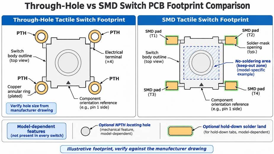
A through-hole switch has leads inserted into drilled holes, normally plated where electrical connections are required. The footprint must specify finished hole diameters, terminal spacing, annular rings and seating position. Check the largest permitted lead dimensions against drilling and plating tolerances. Tight holes can prevent insertion; excessive clearance can complicate placement and solder filling.
An SMD switch generally replaces electrical lead holes with copper lands. Pad geometry, solder-mask openings and stencil apertures must match the termination shape. Gull-wing, J-bend and bottom-contact terminals can require different footprints even when their switch bodies look similar.
Mechanical details deserve separate checks:
• Locating bosses: Plastic positioning features may require non-plated holes.
• Hold-down tabs: Metal retention features may need solder lands or separate holes; their electrical function must be identified from the drawing.
• Terminal orientation: CAD symbols, footprint numbering and physical terminals must agree.
A switch marketed as SMD may still have through-board retention features. These do not necessarily require a separate soldering operation: some are mechanical only, while others may be compatible with a qualified reflow or additional soldering process. Confirm the actual construction with the assembler.
The land pattern also defines areas that must remain clear. Panasonic’s EVP-BL drawing, for example, identifies a no-soldering area and warns that exposed copper or vias there can create solder-ball shorts, uneven seating or flux intrusion. That restriction is specific to the component drawing and must be carried into the released PCB footprint.
2. Check the Internal Terminal Pairs
Many four-terminal tactile switches contain two internally connected terminal pairs. If a footprint is rotated or numbered incorrectly, the PCB can unintentionally connect two circuit nodes through a permanently joined pair. The input may then appear closed without a button press.
For a conventional two-pair tactile switch, designers may choose diagonally opposite terminals to reduce sensitivity to a 90-degree rotation. This practice must be verified against the exact switch circuit diagram, since pin arrangements differ by model. Check the manufacturer drawing before approving the symbol-to-footprint mapping and production orientation.
3. Confirm the Board Assumptions in the Datasheet
Switch drawings sometimes presume a particular PCB thickness or construction. Omron’s published tactile-switch precautions, for example, describe a 1.6 mm single-sided PCB design basis and warn that changes in thickness or hole construction can affect mounting and soldering. This is a manufacturer-specific precaution, not a default requirement for all switches.
Check board thickness, plated-hole construction, local copper distribution and mounting stability against the chosen part’s instructions. A switch evaluated on a prototype board may require fresh verification when moved to a different production stack-up.
4. Design the Mechanical Load Path
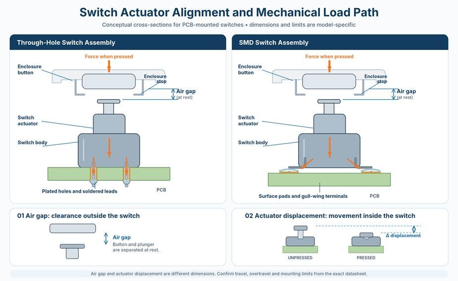
A button press transfers force through the actuator, housing, mounting features and PCB. With many SMD parts, some load reaches solder joints and copper pads. Through-hole leads can transfer load through soldered barrels. Actual retention depends on the component geometry, board support and enclosure design.
Force direction matters. Off-centre pressing or repeated lateral loads can damage a switch or stress its joints. Omron cautions against angled actuation in its tactile-switch guidance, while Panasonic’s EVP-BL precautions warn against side loading and unwanted contact with the enclosure button during assembly. Such precautions must be interpreted for the exact model.
Check the full mechanical stack-up: PCB position, actuator height, operating point, available travel, enclosure variation and board deflection. If the design permits excessive travel, consider an enclosure stop or support. Neither mounting style guarantees durability without suitable mechanical integration.
5. Choose the Production Route Before Layout Release
A board assembled mainly by SMT may need an additional process for through-hole switches. Depending on the part, this may involve insertion and wave, selective or hand soldering. A compatible through-hole component can sometimes use pin-in-paste reflow, but the process must be qualified rather than assumed.
Three manufacturing questions should be answered early:
• Is there enough solder volume? Typical solder paste contains approximately half its volume as solder metal. Pin-in-paste design therefore requires a solder-volume calculation. Overprinting, stencil modifications or solder preforms may be needed, subject to nearby component clearances.
• Can selective soldering reach the joint? Nozzle clearance depends on neighbouring component height, spacing and accessibility. Confirm these limits with the EMS provider before freezing the layout.
• Is the switch approved for the process? Reflow temperature, allowable soldering cycles, cleaning and handling restrictions vary by model. Omron publishes different precautions for its tactile-switch families; its limits must not be extended to unrelated parts.
For production handoff, record the accepted soldering method, thermal profile, permitted exposures, cleaning restrictions and post-solder checks. A sound-looking solder joint does not establish correct switching performance.
6. Match Inspection to the Mounting Method
For SMD switches, assess alignment, seating, terminal wetting, bridging and hold-down joints. For through-hole switches, examine lead insertion, protrusion, solder fill and solder-side clearance. Specify the applicable IPC-A-610 revision and acceptance class, together with any customer-specific criteria, rather than applying an arbitrary universal hole-fill percentage.
Functional inspection should verify that the actuator returns freely, ON and OFF states operate through the intended circuit, and the installed enclosure does not create unintended loading. Additional cycling, environmental or electrical tests should follow the product’s risk and qualification plan.
First article inspection must also confirm part number, drawing revision, terminal orientation and assembly configuration.
7. Control the Change from Through-Hole to SMD
Consider an OEM moving from a through-hole tactile switch to an SMD version to reduce assembly steps. The contact function may appear equivalent, but a controlled review is still necessary:
• Electrical: Confirm contact configuration, internal terminal pairing, rated load and switching behaviour.
• PCB: Release the correct pads, holes, keep-outs, fabrication drawings and placement data.
• Mechanical: Recheck actuator position, alignment, travel, board stiffness and load path.
• Manufacturing: Validate soldering compatibility, packaging orientation, fixtures, cleaning and inspection.
• Qualification: Compare production-representative samples, record test results and approve exact part and PCB revisions.
For procurement teams evaluating alternative suppliers, these gates provide a useful framework for second-source switch evaluation. Matching headline ratings or package dimensions alone does not establish interchangeability in a finished product.
PCB Release Checklist
Before approving a revised switch, confirm that the engineering, purchasing and manufacturing teams agree on:
• Component identity: Complete part number, drawing revision and approved alternatives.
• Footprint: Pads, holes, locating features, hold-downs, keep-outs and pin mapping.
• Board construction: Thickness, layers, hole type and assumptions stated in the datasheet.
• Mechanical interface: Actuator height, operating position, travel, enclosure clearance and support.
• Assembly process: Approved soldering method, process access, cleaning and inspection limits.
• Verification: First article inspection, electrical checks and any required reliability testing.
• Change control: Documented engineering and purchasing approval before substitution.
The best mounting option is one the whole assembly can manufacture and operate consistently. Both through-hole and SMD switches have appropriate roles, including on mixed-technology boards.
For an initial review of mounting options, engineers can examine Swiclick’s tactile switch range and request model-specific drawings for their own PCB evaluation.